

Thermal management.
Crystals that carry heat away.
A thermal management campaign finds substrate and heat-spreader crystals that pull heat away from your chip while keeping the circuit electrically insulated.
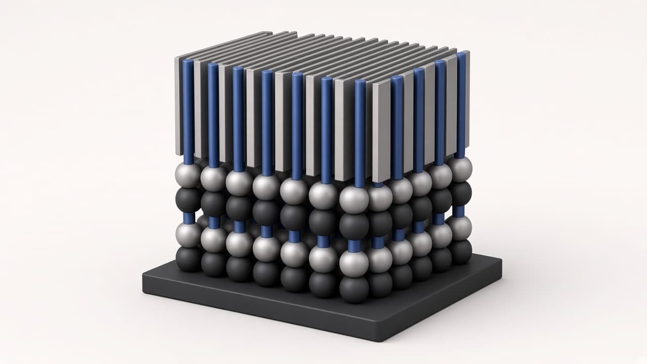
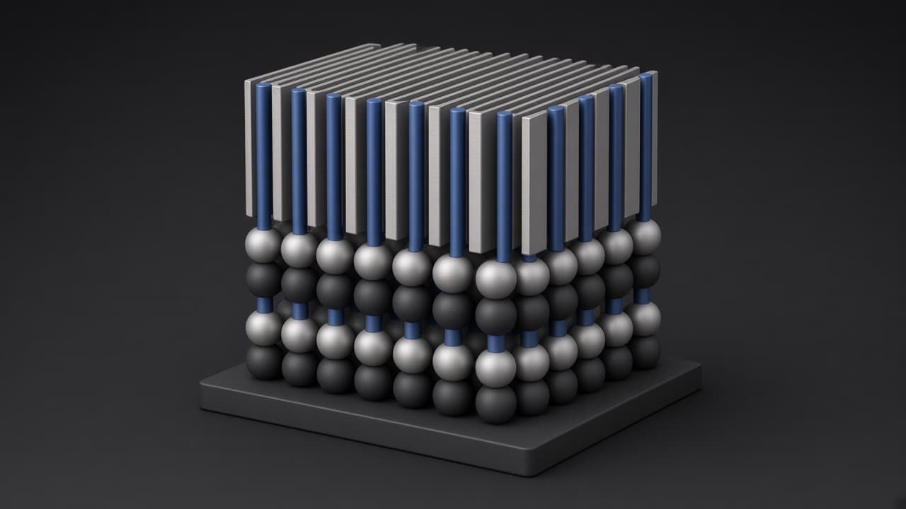
- Power-module substrates
- LED and laser packages
- RF device packages
Why this domain matters to your work.
Thermal management materials decide how much power a device can handle before its own heat limits it. Every power module, LED, laser and RF package sits on a substrate or spreader that has to pull heat away from the chip quickly while keeping the circuit electrically insulated. AlN, silicon nitride, sapphire, silicon carbide and diamond each fill part of that role, and as devices shrink and switch more power, the substrate becomes as important to reliability as the chip on it.
The ideal heat spreader conducts heat like a metal, insulates like a ceramic, expands with temperature as silicon does and costs little, and no single crystal does all four. Diamond and cubic boron nitride conduct superbly but are expensive and hard to make in large pieces. AlN balances conduction and insulation, silicon nitride brings toughness at lower conductivity, and RF packages also need a low dielectric constant. Each choice trades conductivity against insulation, expansion match, permittivity, cost and supply.
With a campaign, you specify the thermal conductivity, the electrical insulation, the expansion match to the chip, the dielectric constant and cost, and receive ranked nitride, III–V, group-IV, oxide and silicon nitride crystals with estimated room-temperature thermal conductivity, insulation, expansion match to silicon, dielectric constant and cost. Conductivity is estimated for a perfect crystal. Grain boundaries, defects and impurities in a real ceramic lower it, and interface resistance, breakdown strength and behavior above room temperature need measuring.
The material families this domain searches.
Each family brings its own structures and chemistry to the search. A campaign can search one of them or compare several under the same targets.
Wurtzite nitrides
AlN and its alloys, insulating ceramics that conduct heat well, chosen as the standard heat spreader under power modules and LEDs.
Zincblende III–V compounds
Boron arsenide, cubic boron nitride and their relatives, chosen when a device needs some of the highest thermal conductivities known.
Group-IV crystals
Diamond, silicon carbide and silicon, chosen for very high thermal conductivity, with diamond at the top and silicon as the low-cost baseline.
Corundum oxides
Sapphire and its substitutions, chosen for a hard, insulating and widely available substrate where moderate heat flow is enough.
β-silicon nitride and SiAlON
Silicon nitride substrates and their sialon form, chosen when toughness matters under repeated heating and cooling, at lower conductivity than AlN.
The properties a campaign can aim for.
Choose the properties that matter to your work. For each one, say whether a candidate must meet it or should push it as far as it goes, with cost and supply always in view.
- Thermal conductivity at room temperature
- Electrical insulation
- Expansion match to silicon
- Low dielectric constant
- Cost and supply risk
Starting points for a campaign.
Each starting point sets up a campaign for a common goal in this domain. Begin from one and adjust its targets, or set your own from the start.
Insulating heat spreaders
Suits power-module designers, searching for AlN-class substrates that conduct heat well and keep the circuit insulated.
Ultra-high-conductivity crystals
Suits devices limited by heat above all, ranking diamond, SiC, c-BN and BAs-class spreaders on conductivity first.
Low-cost substrates
Suits high-volume products, searching for substrates built from common elements only, under a tight budget.
RF and low-loss packages
Suits RF package designers, searching for low-permittivity crystals that keep signal loss low while carrying heat away.
What you specify, what you receive and where the figures stop.
MS Lattice hands your lab a shortlist to make and test. Its figures are screening estimates and calculations, not measurements of the new material, and each domain says where they stop.
You specify
The thermal conductivity, the electrical insulation, the expansion match to the chip and the dielectric constant you need, and cost.
You receive
Ranked nitride, III–V, group-IV, oxide and silicon nitride crystals, with estimated room-temperature thermal conductivity, insulation, expansion match to silicon, dielectric constant and cost.
Before you rely on it
Conductivity is a screening estimate for a perfect crystal; grain boundaries, defects and impurities in a real ceramic lower it. Interface resistance, breakdown strength and behaviour above room temperature need measuring.
The same four modes work in every domain.
Search from your targets alone, improve a material your team already uses, or watch the engine reach known materials, with the targets as guides or sealed away, to see how well it searches.
Open Discovery
Choose it when you know what the material must do but have no starting structure.
Prototype-Guided Optimization
Choose it when you already have a good material and want to make it better.
Guided Rediscovery
Choose it when you want to watch the engine reach a material you already know.
Blind Rediscovery Benchmark
Choose it when you want to test whether the engine finds an answer it was never shown.
Every candidate arrives with its record.
Each candidate comes ranked against your targets, with its estimated properties and their uncertainty, the checks it passed and a structure file to export, ready for your lab.
Questions teams ask about this domain.
Have a materials target? Tell us what it must do.
Share the material domain, the properties you need and the limits the material must respect. We will show you how MS Lattice would approach it through Norck, from a ranked shortlist for your own lab all the way to finished parts.