Why power electronics is a materials problem
Every electric vehicle inverter, fast charger, solar inverter and data-center power supply converts electricity by switching it on and off very quickly. Switch at a higher voltage and you move the same power with less current and less copper. Switch at a higher frequency and the inductors, capacitors and transformers around the switch get smaller. Do both with lower losses and the whole converter shrinks, runs cooler and costs less to cool.
Silicon has carried the industry for decades, but it is close to its limits for high-voltage switching. Silicon carbide and gallium nitride have moved into production for this reason, and gallium oxide, aluminium-rich nitrides and diamond sit further out. A smaller, faster switch concentrates more heat in less area, so the materials around the die matter as much as the die: the substrate that insulates it and carries heat away, the crystals that time and filter its signals, the optics around it and, sometimes, a solid-state cooler.
MS Lattice covers that stack with five domains. Each is a separate campaign with its own targets, and each says where its figures stop.
Wide-bandgap semiconductors: the switch itself
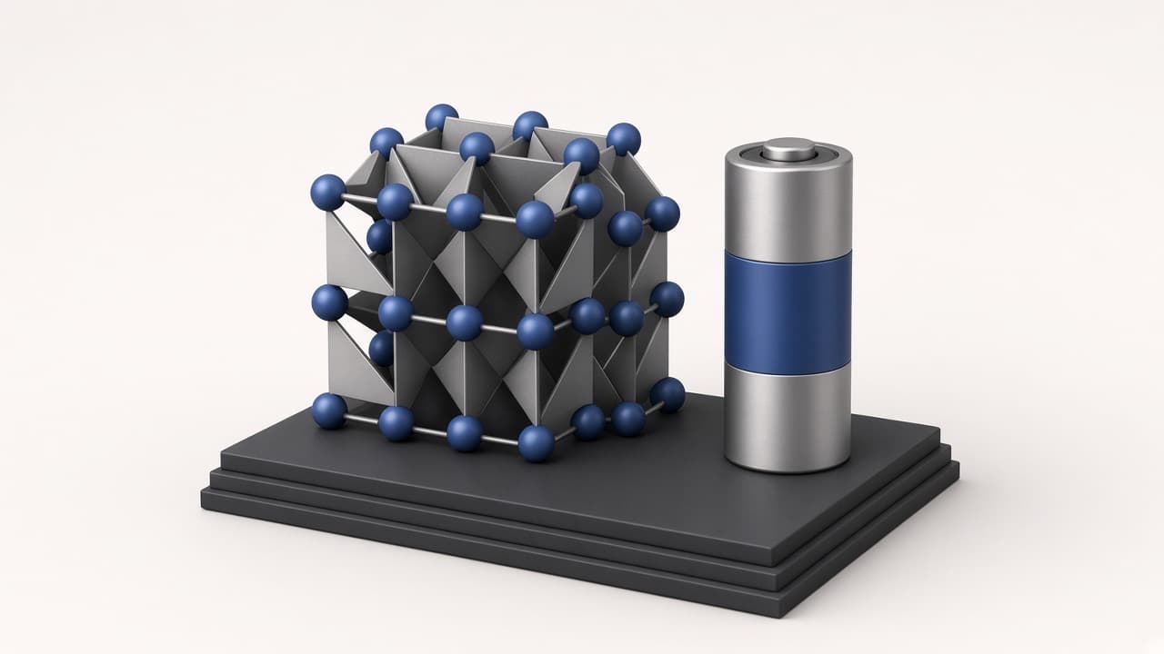
A wider band gap lets a semiconductor withstand a stronger electric field before it breaks down. For a power switch that means a thinner, more heavily doped drift layer for the same voltage, and so lower resistance when the switch is on. The Baliga figure of merit is the standard way the industry ranks materials on that trade-off for power devices. Band gap alone is not enough, though. Gallium oxide has a very wide gap but conducts heat poorly and is hard to dope p-type. Diamond is outstanding on paper and hard to grow and dope in practice.
That is why the domain aims for six things together: a band gap from 3 to 6 eV, the Baliga figure of merit, electron mobility, thermal conductivity, dopability, and cost and supply risk. Its groups are β-gallium oxide, with aluminium and indium; wurtzite AlGaN, for GaN power and RF devices and AlGaN deep-UV emitters; boron nitride, cubic and hexagonal, the widest gaps here; and group-IV crystals, silicon carbide and diamond with boron.
Four starting points match the main device classes: Power switching, for SiC, GaN and Ga₂O₃-class switches; RF power, for GaN-class transistor channels; Deep-UV optoelectronics, for UV emitters and solar-blind detectors; and Low-cost power semiconductors, which keep to SiC, diamond and boron nitride, without gallium or indium. Gallium supply is concentrated, so that last option is a real choice for programs worried about it. You specify the band gap, the device class, the figure of merit you need and the elements you can source.
Thermal management: getting the heat out
A power die sits on a ceramic substrate that must do two jobs at once: insulate the die electrically from the cooling system and conduct its heat away as fast as possible. Aluminium nitride conducts heat well, silicon nitride is tougher and survives power cycling better, and alumina is the low-cost default. Each heats and cools thousands of times in service, and a mismatch in thermal expansion between die, substrate and metal layers is a classic cause of cracked joints and lifted bonds.
The thermal-management domain searches wurtzite nitrides such as AlN and its alloys; zincblende III–V compounds, boron arsenide, cubic boron nitride and their relatives; group-IV crystals, diamond, silicon carbide and silicon; corundum oxides, sapphire and its substitutions; and β-silicon nitride and SiAlON. Its targets are thermal conductivity at room temperature, electrical insulation, expansion match to silicon, a low dielectric constant, and cost and supply risk.
The starting points split the field the way package engineers do: Insulating heat spreaders, AlN-class substrates for power modules; Ultra-high-conductivity crystals, from diamond and SiC to c-BN and BAs-class spreaders; Low-cost substrates, common elements only; and RF and low-loss packages, low-permittivity crystals for RF substrates. AlN appears here and again in the piezoelectric domain, a reminder that one crystal can serve two layers of the same product.
Piezoelectric and dielectric crystals: timing, filtering and sensing
Power and RF systems depend on crystals that convert between electrical and mechanical energy. Quartz sets the clock for the controller. Thin-film AlN and scandium-doped AlN resonators filter RF signals. Piezoelectric sensors and actuators sit near motors and hot spots. The established actuator ceramic, lead zirconate titanate, contains lead, and pressure to remove lead from electronics is long-standing.
MS Lattice’s domain leaves lead-containing compositions out. It searches ferroelectric perovskites, BaTiO₃ and (K,Na)NbO₃; wurtzite nitrides and oxides, AlN, scandium-doped AlN and ZnO films for resonators; quartz-type crystals, quartz and GaPO₄, for frequency control and hot sensors; and LiNbO₃-type crystals for surface-acoustic-wave and high-temperature transducers. It aims for the piezoelectric coefficient, the depolarization temperature, electromechanical coupling, electrical insulation, and cost and supply risk.
Depolarization temperature deserves a place in any brief for power hardware. A piezoelectric ceramic that loses its polarization near a hot module stops working, so the temperature it must hold belongs in the requirements, not the preferences. The High-temperature sensor crystals starting point is built for that case.
Optical materials and thermoelectrics: light and heat at the edges
Optical materials come in where light enters or leaves a system. Transparent conducting oxides, ITO, doped ZnO and doped SnO₂, serve as electrodes for displays, touch panels and solar cells, and doped ZnO and SnO₂ avoid indium. Zincblende and diamond windows, ZnS, ZnSe, GaP and germanium, serve infrared optics such as the thermal cameras used to find hot spots on a running board. Fluoride and alkali-halide windows reach from the ultraviolet to the far infrared. The domain also covers inorganic scintillators, which are outside a power stack. It aims for the infrared cutoff, film resistivity or light yield, moisture resistance, visible transparency, scintillation timing, stopping power, and cost and supply risk.
Thermoelectrics turn a temperature difference into power, or a current into cooling. In electronics they appear as solid-state coolers that hold a laser diode or detector at a set temperature, and as generators that recover waste heat. The domain searches chalcogenides, skutterudites, half-Heuslers and oxides, and aims for the figure of merit (ZT), power factor, low thermal conductivity, operating temperature and element cost, with Maximum ZT, Lead-free and Waste heat as starting points. Note the inversion: a heat spreader wants the highest thermal conductivity it can get, and a thermoelectric wants the lowest.
How the domains meet in one device
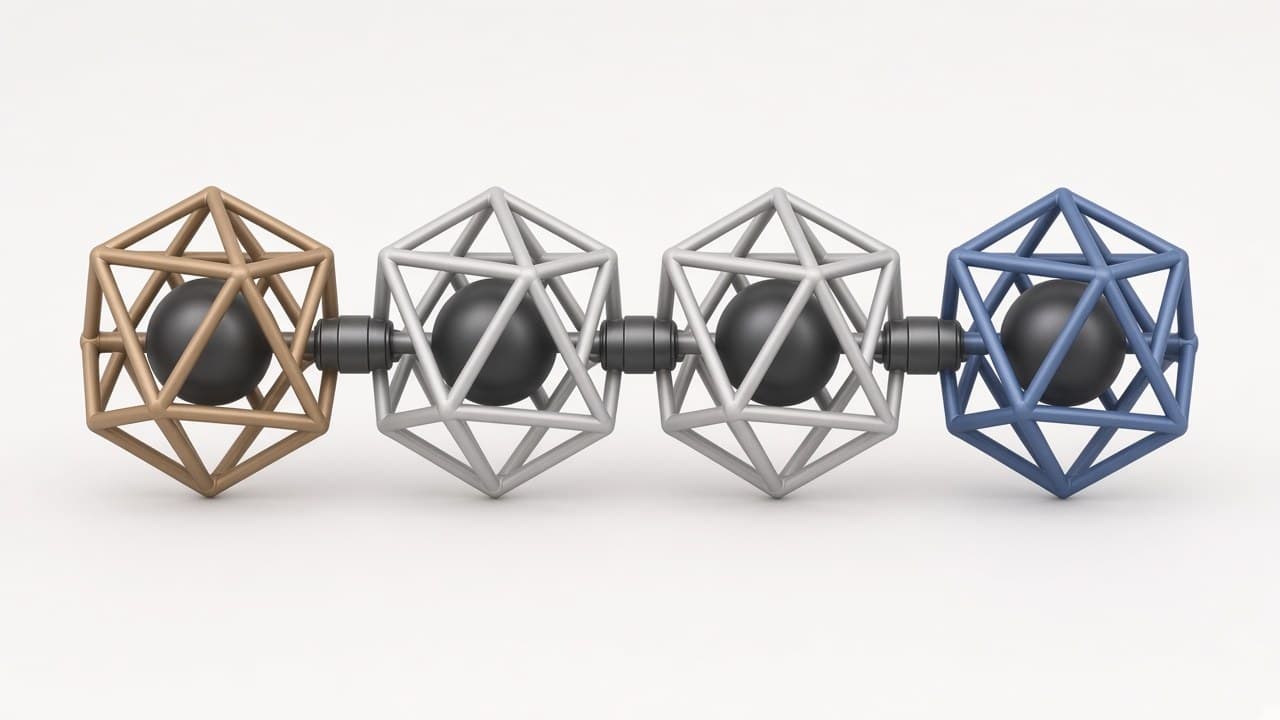
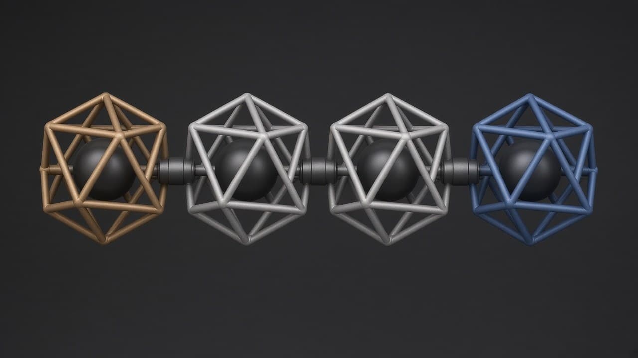
Follow a power module from the die outward and the domains line up, along with the layers no domain covers:
- The dieA wide-bandgap campaign ranks the switch material on band gap, figure of merit, mobility, thermal conductivity and dopability.
- The insulating substrateA thermal-management campaign ranks the ceramic under the die on conductivity, insulation and expansion match.
- The joints and the cold plateSolders, sintered layers, interface materials and the cooler are outside these domains. They are chosen and tested in the package.
- Timing, filtering and sensingA piezoelectric campaign ranks lead-free crystals for clocks, resonators and sensors that must hold their response at temperature.
- Light and local coolingOptical and thermoelectric campaigns cover windows, transparent electrodes and solid-state coolers where the system needs them.
Each campaign has its own brief, but the briefs should share constraints. If your program will not depend on gallium or indium, say so in every one. If the product has a maximum service temperature, write it into each domain’s requirements in that domain’s terms.
What you receive, and where the figures stop
Each domain hands back a ranked shortlist with estimates for its own targets, each candidate with its uncertainty, the checks it passed and a standard structure file. The semiconductor domain returns gallium oxide, nitride, boron nitride and group-IV candidates with estimated band gap, Baliga figure of merit, mobility, thermal conductivity, dopability and cost. The thermal-management domain returns nitride, III–V, group-IV, oxide and silicon nitride crystals with estimated conductivity, insulation, expansion match, dielectric constant and cost. The piezoelectric domain returns lead-free candidates with estimated coefficient, depolarization temperature, coupling, insulation and cost.
None of these five domain pages carries a proof of its own on the record. Two general results are close to this reader’s materials. First-principles calculations reproduced silicon’s lattice constant, 5.4745 Å, its three elastic constants and its highest optical phonon, each within the tolerance set before the run. And BaTiO₃, the ferroelectric perovskite in the piezoelectric domain, was one of four compounds held out of everything MS Lattice starts from and rebuilt to within a few hundredths of an ångström. Those are structure and property checks, not semiconductor or piezoelectric figures.
- 5 of 5silicon reference values reproduced
- 4 of 4unseen compounds rebuilt, within 0.016–0.037 Å
Questions teams ask
Can MS Lattice predict a device’s breakdown voltage?
No. It estimates bulk-crystal properties such as band gap and the Baliga figure of merit. Device breakdown, contacts and reliability depend on growth and design and are measured on made devices.
Why is thermal conductivity a target in the semiconductor domain too?
Because the die makes the heat. A wide-gap material that cannot move heat out of the channel limits the device however good its gap is.
Does the piezoelectric domain include PZT?
No. Lead-containing compositions are left out. The domain searches lead-free perovskites, nitrides, quartz-type and LiNbO₃-type crystals.
Can we keep gallium and indium out of every campaign?
Yes. Set the elements you will not use in each brief. In the semiconductor domain, the Low-cost power semiconductors starting point already leaves both out.


MatterSpace’s first domain engine
MatterSpace built MS Lattice for the scientists and engineers who discover and design new materials, starting from the properties their product needs.